A team of researchers at Cnr Nano and Scuola Normale Superiore at NEST Laboratory has demonstrated a groundbreaking approach to managing signals in cryogenic quantum devices, achieving time-division multiplexing (TDM) of non-dissipative supercurrents using hybrid superconducting electronics. Their work, recently published in Nature Communications, paves the way for more compact, efficient, and scalable quantum systems.
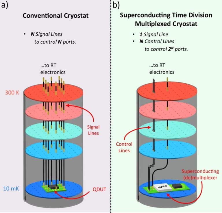
Modern quantum experiments often rely on cryogenic temperatures to maintain coherence and minimize noise. However, controlling multiple quantum devices requires extensive wiring from room temperature down to the coldest stages of a cryostat. Each additional line adds cost, volume, and thermal load, limiting the scalability of quantum setups. Traditional approaches to TDM—using electromechanical switches or cryogenic CMOS devices—face challenges such as large size, slow switching times, power dissipation, and insertion losses, making them less suitable for superconducting qubits.
Alessandro Paghi and Francesco Giazotto’s research group tackled these challenges by developing Josephson Field Effect Transistors (JoFETs) on the InAs-on-Insulator platform. These devices feature aluminum superconducting electrodes and hafnium oxide gate insulators, enabling them to fully switch off the supercurrent while maintaining high non-dissipative currents in the ON-state, making them ideal for superconducting multiplexers.
Using these building blocks, the researchers built a demultiplexer with one input and eight outputs, operating at 50 mK with a signal frequency up to 100 MHz and a switching frequency of 100 kHz. “Remarkably, the device exhibits near-zero insertion loss in the superconducting state and an ON/OFF ratio of ~17.5 dB, establishing a lossless path for supercurrents. By optimizing the on-chip routing, a dual-output demultiplexer was demonstrated to work up to 4 GHz, retaining similarly low loss and high ON/OFF performance”, explains Alessandro Paghi.
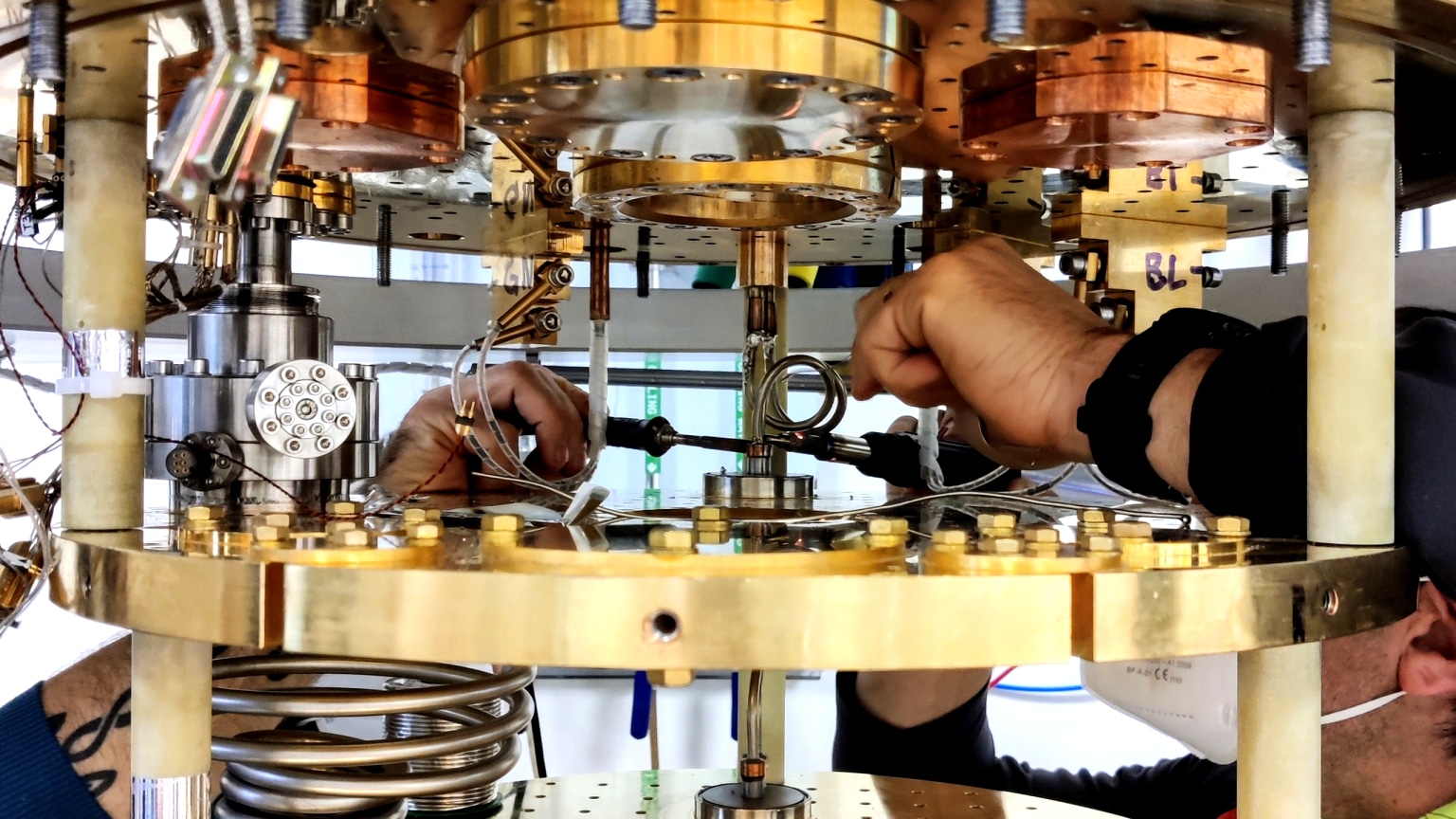
The achievement was made possible thanks to advanced nanofabrication technologies available at Cnr Nano within the NEST Laboratory in Pisa, which enabled the precise integration of superconducting and semiconducting materials at the nanoscale.
This innovative superconducting TDM approach promises to significantly reduce the number of physical signal lines required in cryostats, lowering cost, space, and thermal load, while supporting faster, high-fidelity control of superconducting quantum devices. The work represents a critical step toward scalable quantum technologies, combining the benefits of superconductivity with the compactness and speed of solid-state electronics.
Reference: Paghi, A.; Borgongino, L.; Tortorella, S.; De Simoni, G.; Strambini, E.; Sorba, L.; Giazotto, F. Supercurrent Time Division Multiplexing with Solid-State Integrated Hybrid Superconducting Electronics. Nat. Commun. 2025, 16 (1), 8442. https://doi.org/10.1038/s41467-025-62931-3.


